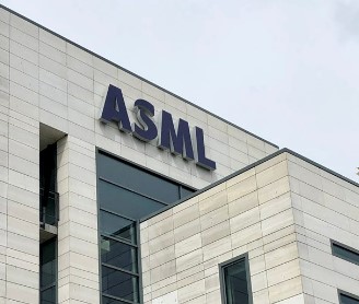
ASML is a Dutch multinational corporation that designs and manufactures advanced technology for the semiconductor industry. The company was founded in 1984 and is headquartered in Veldhoven, Netherlands.
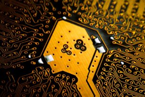
ASML’s primary products are Lithography systems, used by chipmakers to pattern circuits onto silicon Wafers.
These systems use ultraviolet light to shrink the size of features on the Wafers, enabling the production of smaller and more powerful chips.
ASML is one of the leading suppliers of lithography systems in the world, and its customers include major semiconductor manufacturers such as Intel, Samsung, and TSMC (Taiwan Semiconductor Manufacturing Company Limited).

In addition to lithography systems, the company also provides related products and services, such as metrology systems, software, and maintenance.
ASML produces several types of products for the semiconductor industry, including:
Lithography systems: These are used to pattern circuits onto silicon wafers using ultraviolet light. ASML offers several types of lithography systems, including extreme ultraviolet (EUV) and immersion systems.
Metrology systems: These systems are used to measure and inspect the patterns on silicon wafers, ensuring that they meet the required specifications. ASML’s metrology systems include optical and x-ray systems.
Software: ASML provides a range of software solutions to help customers optimize the performance of their lithography systems, including mask synthesis, simulation, and modeling software.
Maintenance and service: ASML offers a variety of services to support customers throughout the lifecycle of their systems, including installation, training, and ongoing maintenance and repair.
DUV – Deep ultraviolet lithography systems, also known as i-line and DUV systems, are used to pattern circuits onto silicon wafers using deep ultraviolet light.
EUV – Extreme ultraviolet lithography systems, also known as EUV systems, are used to pattern circuits onto silicon wafers using extreme ultraviolet light.

These systems are considered the next generation of lithography technology, as they are capable of producing even smaller and more complex patterns than previous systems.
- Website Optimization Secrets: Boost Traffic & Skyrocket Growth!
 SEO Optimization – Identify relevant keywords, optimize meta descriptions, and improve on-page SEO to increase …
Website Optimization Secrets: Boost Traffic & Skyrocket Growth! Read More »
- Understanding the Digital Immune System: Why IT IS Needed
 In our interconnected and digitized world, threats to our digital assets are ever-present. Just as …
Understanding the Digital Immune System: Why IT IS Needed Read More »
- top evergreen holi songs
 ADVERTISEMENT We have sorted for you the best holi songs ever made… let’s see the …
 - Top 5 Text To Image Converter AI Tools For you in 2024
 As AI tools are becoming popular so rapidly finding the perfect text to image converter …
Top 5 Text To Image Converter AI Tools For you in 2024 Read More »
- Top 10 Stocks Where Promoters Increased Their Stakes in 2025 – A Sign of Strong Confidence!
 ADVERTISEMENT In 2025, several Indian companies experienced significant increases in promoter holdings, reflecting strong confidence …
 - Things to know about Semiconductor Giant company : ASML
 ASML is a Dutch multinational corporation that designs and manufactures advanced technology for the semiconductor …
Things to know about Semiconductor Giant company : ASML Read More »
Watch Quick Stories